
PCB Design & Engineering
Multilayer, HDI, rigid-flex, high-speed, RF and mixed-signal PCB engineering for reliable, production-ready electronic systems.
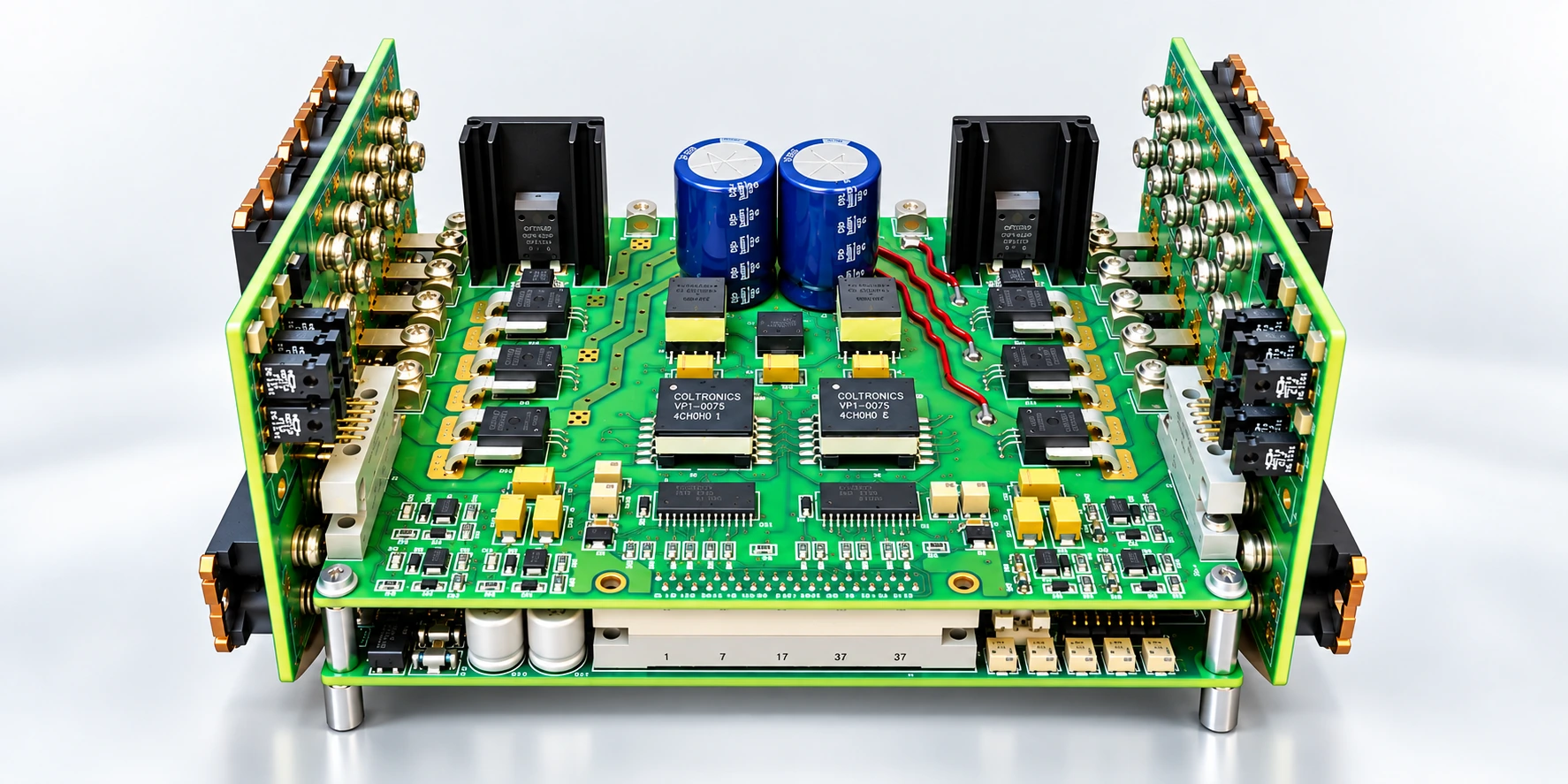
Overview
RTS provides PCB design and engineering for complex aerospace, defence and electronic-system requirements, supporting multilayer, HDI, rigid-flex, high-speed, RF, mixed-signal and high-current designs. The division addresses the complete design flow from schematic inputs and stack-up definition through component placement, routing, engineering analysis, design verification and fabrication-ready outputs.
PCB engineering capability includes controlled-impedance and critical-signal routing, fine-pitch and high-pin-count BGA layouts, signal-integrity analysis, power-integrity and power-distribution-network analysis, thermal analysis, EMI/EMC-aware design and DFM, DFA and DFT assessment. RTS also supports PCB re-engineering and layout conversion for existing electronic systems.
PCB Design & Engineering Capabilities
PCB Architecture & Layout
Schematic Capture & PCB Architecture
Translation of circuit and system requirements into schematic definitions, PCB architecture, stack-up planning and implementation strategy.
Multilayer & HDI PCB Design
Design of complex multilayer and high-density interconnect PCBs for dense, space-constrained and high-performance electronic systems.
Rigid-Flex PCB Design
Rigid-flex board design for compact assemblies requiring mechanical flexibility, reduced interconnects and constrained packaging.
Fine-Pitch & High-Pin-Count BGA Design
Component placement, escape routing and layout engineering for fine-pitch and high-pin-count BGA devices.
High-Speed, RF & Power Layout
High-Speed & Controlled-Impedance Design
High-speed PCB layout with controlled impedance, differential routing and critical-signal management for demanding digital interfaces.
RF & Mixed-Signal PCB Design
Layout and routing for RF, analogue, digital and mixed-signal circuits with attention to isolation, return paths and signal integrity.
High-Current & High-Voltage PCB Design
PCB layout for elevated current and voltage requirements, considering conductor sizing, spacing, power distribution and thermal behaviour.
EMI/EMC-Aware Layout Engineering
Placement, routing, grounding and layout practices intended to reduce electromagnetic interference and support EMC performance.
Simulation & Engineering Analysis
Signal Integrity Analysis
Analysis of crosstalk, reflections, impedance behaviour and signal quality to optimise high-speed and sensitive signal paths.
Power Integrity & PDN Analysis
Analysis of voltage drop, current distribution, impedance and power-distribution-network behaviour to support stable board-level power delivery.
Thermal Analysis
Thermal evaluation of PCB layouts to identify hot spots, assess heat distribution and support component placement and heat-dissipation decisions.
DFM, DFA & DFT Analysis
Design-for-manufacturability, assembly and test analysis to improve production readiness, accessibility and repeatability.
Re-Engineering & Production Readiness
PCB Re-Engineering & Layout Conversion
Re-engineering of existing boards and migration or conversion of PCB layouts to support redesign, obsolescence management and continued production.
CAM, Gerber & Fabrication-Ready Outputs
CAM verification, manufacturing-data generation and fabrication-ready output preparation supporting transition from completed layout to PCB fabrication.